This is the first post on my power supply build. Also see part II and the Circuitmaker project page.
An adjustable bench power supply has been on my list of things to build for quite a while. A linear supply should be relatively simple to design, with the added bonus of being a useful thing to have around. My goals with this project are to design and build a slightly more complex system than I have in the past, to lean to use PCB layout software and to actually get a PCB designed and manufactured. I wanted to design it from scratch, rather than using an adjustable 3 terminal regulator or a controller chip with everything built in – this is supposed to be a learning experience more than anything else.
My requirements are:
- 0-30V adjustable voltage
- 0-2A with current limiting.
- Separate fixed 5V output for powering digital circuits.
I decided on a digital display for simplicity and compactness on the front panel and so that I can display both the setpoints and measured values. The current and voltage adjustment however are analogue, controlled by pots on the front panel, rather than controlling it digitally with a microcontroller, again for simplicity.
For the schematic and layout I used the new Altium circuit maker, which I plan to do a write up on in a separate post. When I first started thinking about this build many months ago I was using KiCad because it is open source and seems to have a decent following. It is also apparently under fairly active development due to being picked up by CERN a couple of years ago. However, it feels very unpolished and quirky and I was instantly sold on circuitmaker as an alternative when I first tried it.
Design
Searching online I found a few good references which I have based my design on. Kerry Wong’s dual tracking supply is a very good writeup and I have based my design fairly closely on that (part 1, part 2, part 3).
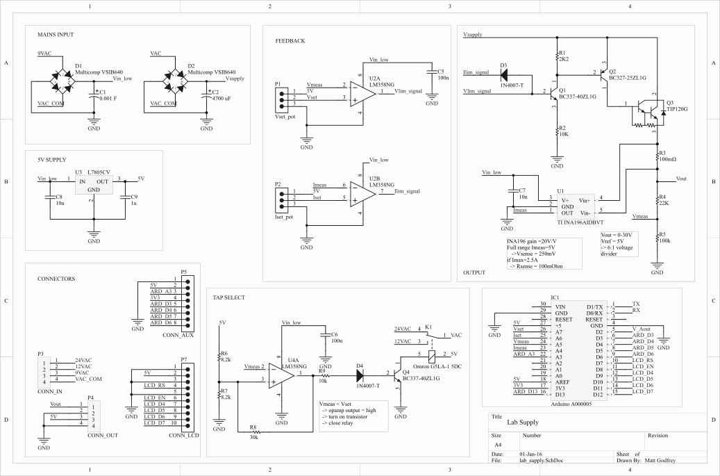
The design is fairly simple and uses a single npn Darlington transistor Q3 (TIP120) as the pass transistor. It is in a common collector configuration and so provides current gain but no voltage gain. Voltage gain is provided by Q1 which is a common emitter configuration. The output voltage is divided down to a 0-5V signal by resistors R4 and R5 to provide the voltage feedback to opamp U2A (LM358), and U1 (INA196) is a current monitor chip which measures the voltage over shunt resistor R3 to provide the current feedback. There is additional circuitry for the mains rectification, the transformer tap select, fixed 5V output and auxiliary power supplies for the different chips.
Voltage control
The main feedback loop is shown below. Opamp U2A has it’s non-inverting input connected to the wiper of a pot on the front panel, driven by a 5V reference signal which provides the setpoint between 0V and 5V. The inverting input comes from the 6:1 voltage divider R4/R5 which also gives a voltage in the range of 0-5V. The output voltage is amplified by the common emitter amplifier created by R1, R2 and Q1, with the pnp transisor Q2 required as the common emitter amplifier is inverting. The current gain is then provided by Q3.
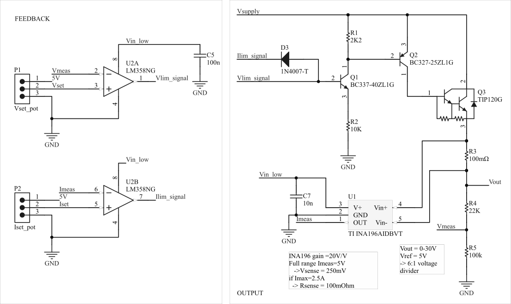
The operation is as follows:
- If the output voltage is larger than the setpoint voltage, U2A output drops low.
- This reduces the base voltage into transistor Q1, reducing the collector current
- This causes the collector voltage to increase (V=IR through resistor R1)
- This reduces the base-emitter voltage at Q2 and reduces the collector current
- This in turn reduces the base current into Q3 which reduces the output voltage
There are a few things to note about this. Firstly, it would be possible to drive the pass transistor Q3 directly with the opamp U1 without dividing the output voltage and without the need for the voltage gain provided by Q1 and Q2. This would simplify the design somewhat but there are a few reasons why this is not a good idea.
- I would still need to divide the output voltage down to be sampled by the microcontroller for display
- This provides more flexibility in the choice of opamp since it only needs to be low voltage
- I would need to generate a reference voltage at 30V which is harder than a 5V one.
The second point is the choice of resistors R1 and R2. They must be chosen such that when transistor Q1 is fully switched on they are not dissipating more than their rated 1/4W. Vcc=30V which means that the total resistance must be at least 3K6 (P=V^2/R). There is a second requirement that the opamp (LM358) is not rail-to-rail and can only pull down to ~1V. In the current limiting circuit there is an also an additional 0.7V drop over the diode D3. So, in order to fully turn off Q1 we need a larger resistance for R2 than R1, so that the emitter voltage is raised up above ground. I have chosen R1=2K2 and R2=10K .
Current limiting
The output current is monitored by measuring the voltage drop over the shunt resistor R3. This is achieved with U1 (TI INA196) which is a dedicated current shunt monitor – basically a differential amplifier with a gain of 20V/V. With a 100mΩ resistor at 2A this develops 200mV, which means the output is in the range from 0-4V. This is fed into the negative input of opamp U1B, with the positive input coming from a second pot on the front panel. This is also connected to the base of transistor Q1 along with the output of the voltage feedback via a diode. When the measured current is lower than the set point, the opamp output is high, the diode is reverse biased and no current flows. If the measured current is above the set point, the opamp output goes low, the diode starts conducting and shuts off Q1 which turns off the main pass transistor.
Mains input
The transformer I selected has 2 windings rated at 2.5A, each with a 9V and 12V tap. The two windings are connected on series to provide 3 AC voltages of 9V, 12V and 24V. The 21V tap is unused. The 9V is rectified and filtered and supplies a 7805 5V regulator. This is used to power the Arduino, the display and the transistor tap select relay. It also provides the fixed 5V output on the front panel.
The main voltage supply is selected from the 12V or 24V tap, bridge rectified and filtered. The tap is selected by relay K1. Opamp U4A is set up as a hysteresis comparator via resistors R6, R7 and R8. The trip point is set at 10V +- 2V. The output from the opamp drives the base of transistor Q4 which switches the relay coil current on or off to select the correct tap. Note resistor R9 limits the base current into Q4, and diode D4 is required as the LM358 can only pull its output down to ~1V which is not enough to switch off Q4. D4 drops an extra half a volt or so which is enough to switch off Q4.
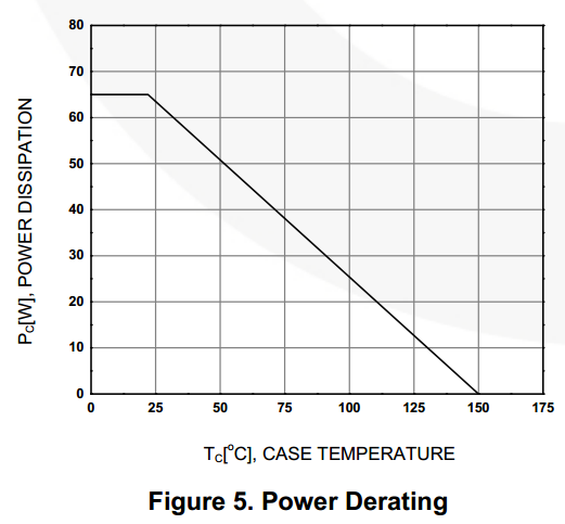
A multi-tap transformer is needed to reduce the power dissipation in the main pass transistor. The worst case in terms of power dissipation is a short circuit, when the full voltage is dropped over the pass transistor at maximum current. With 30V at 2A this gives 60W, which is outside the spec of most transistors. The transistor used in this design (TIP120) has maximum dissipation of 65W at room temperature, but this is reduced to 30W by 80 degrees where it is likely to be operating. This is especially true since I am using a relatively small heat sink and no fan. By using 2 taps, I limit the maximum power dissipation to around 30W , at the expense of the extra complexity of the tap selection circuitry.
Display
Display is handled by an Arduino nano, which measures the setpoint and actual voltages and outputs to a 20×4 character LCD on the front panel. I use the internal ADC on the Arduino, which is 10bit, giving 1024 different values. At 30V and 2A this gives about 30mV and 2mA resolution which is more than enough for my purposes. The code is very simple, shown below. The only slightly tricky part is calibrating the measured values. I have done this by simply measuring the output with a multimeter and adding a multiplicative factor in the code to make the measured and actual values agree.
https://gist.github.com/b389f9d20d11c400ffe1
Layout
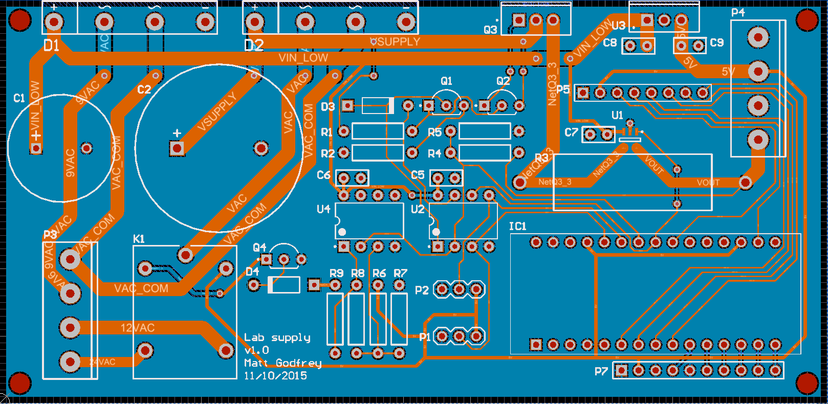
This is the first PCB that I’ve properly laid out so it was very much a learning experience. My major concern was that I don’t have a reference for how important different best-practices are – how much of a problem long winding traces are, how close feedback resistors need to be to the opamp, how wide to make tracks, etc. I think in hindsight I worried about this too much, I feel like it is a fairly simple board that is going to be fairly tolerant to sub-optimal layout. I think I also prolonged the process by trying to fit everything into a relatively small area. The board width was determined by the heatsink I had available (~120mm) and I set the depth at 60mm when in reality there is a lot of spare room in my enclosure.
Manufacture
I had my boards manufactured by PCBWay which I found after a bit of a search online. It is a Chinese company which was very cheap (US$22 + shipping for 5 2 layer boards) and had some good reviews online. The turnaround time was amazingly fast – less than a week between submitting the order and delivery for the standard/cheap shipping option.
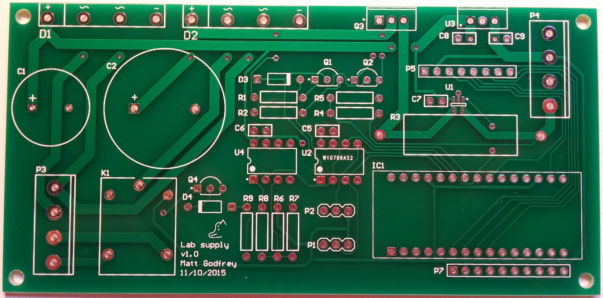
The board quality looks good (to my untrained eyes anyway) and there are no manufacturing problems that I have been able to identify yet. I’ve since found a few small issues with my design and one of the footprints is missing a pad, but these are fixable and I’ll go through them in the next post.
Part II
Part II of this post will follow once I have actually finished building the supply. It will cover the physical build and the enclosure, some of the problems I found with the design and the layout once I actually tested it and some testing. Hopefully this will be finished in the next couple of weeks. I’m also planning a third post looking in more detail at the design and some simulations.
Until next time!


One comment