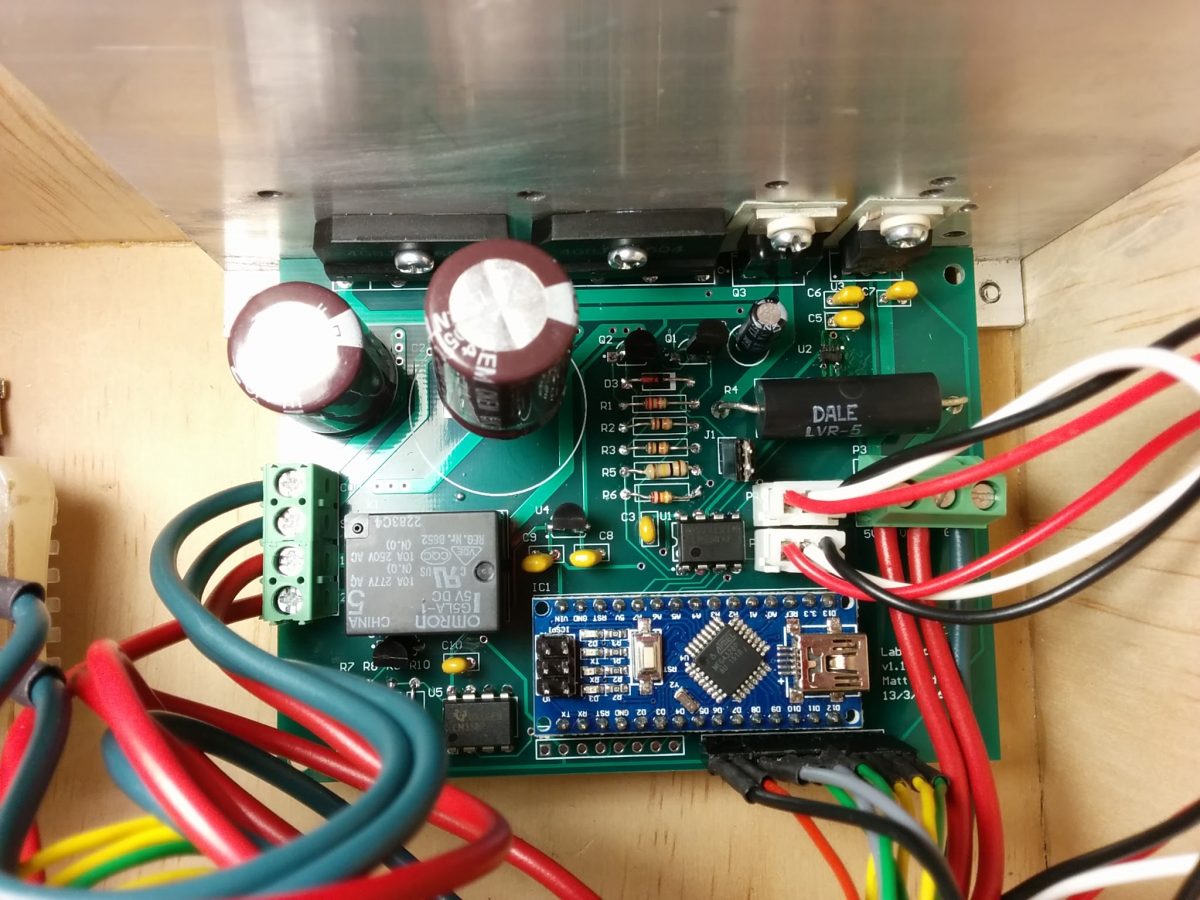
This is the second post on my power supply build – also see part I and the Circuitmaker project page. The aim of this project is to design and build a linear bench power supply with adjustable current and voltage and up to 2.5A output from 0-30V.
After building and testing the first version of the board I discovered a couple of issues. Most of the basic functionality worked – the voltage control, digital display, transformer tap select, etc. However, the current limiting never worked properly, there were some noise/oscillation issues and a couple of mechanical problems. So, Rev.1.1 was born which has now been tested and seems to be working nicely.
This post will go through some of the problems encountered in the first revision of the board and the changes that have been made to this one. I will save a full writeup of the build, the enclosure and some testing for a future post. A description of the operation of the power supply can be found on the Circuitmaker project page here.
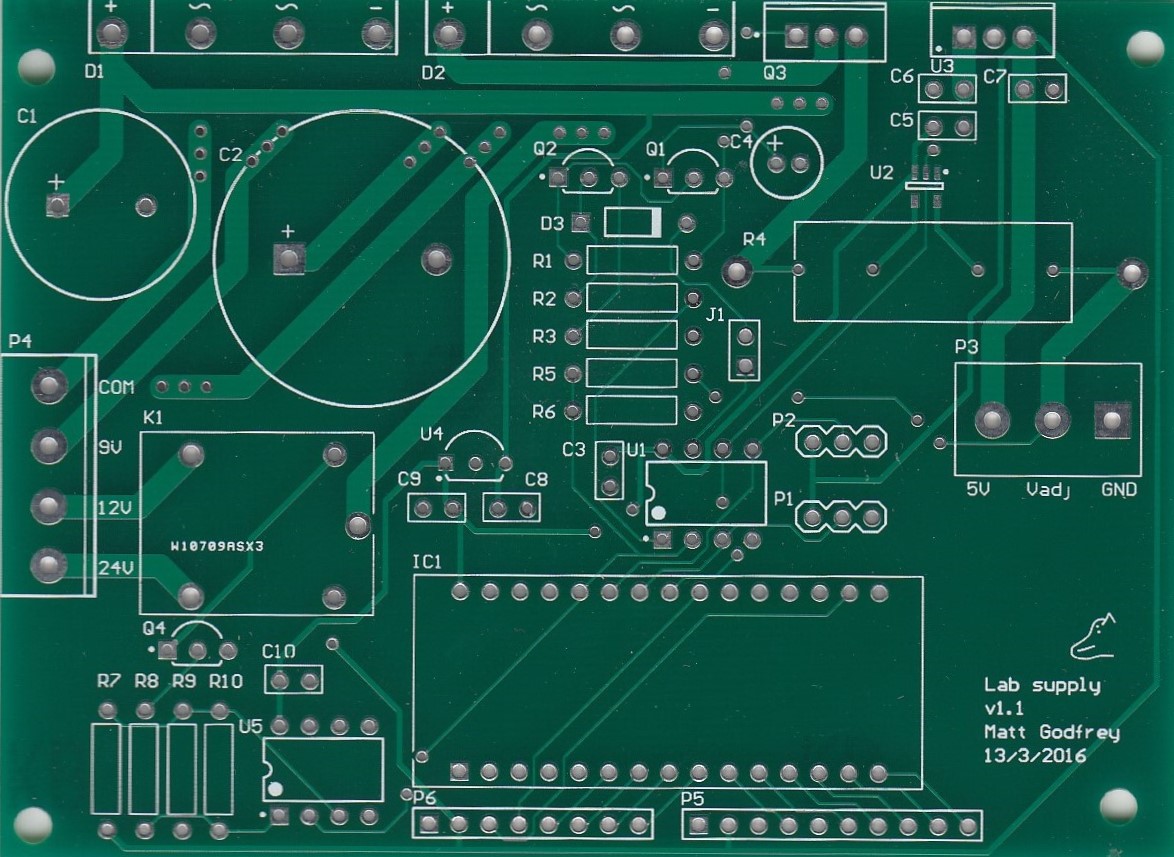
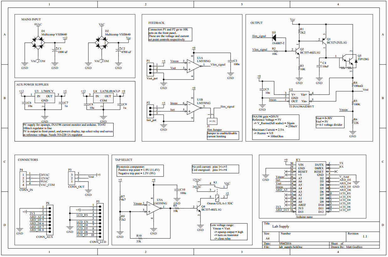
Changes in Rev.1.1
First up, the major changes in Rev.1.1:
- The opamps and current monitor are now powered from a regulated 9V rail.
- Added a current limiting resistor to the output of the voltage feedback opamp for when the supply goes into current limit mode.
- Added a capacitor to the base of the main pass transistor to prevent oscillation.
- Removed the series diode in the tap select circuit.
- Mechanical changes including board shape, component positioning, connectors.
- Complete re-layout of the board. Increased track width and added additional via stitching to high current traces.
- Labelling on the silk screen
Details of changes
Current limiting
On the original board the current limiting never worked with the INA196 current monitor chip (U2) always outputting zero volts. My guess is that the the chip was blown due to an overvoltage on its power pin. This was caused by a separate problem where this power rail (nominally ~12V) reached up to ~35V, well above the 18V rating of the INA196.
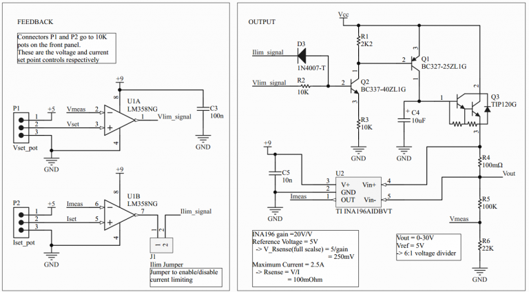
This power rail on the original board was unregulated and taken directly from the 9VAC transformer winding, full fridge rectified and filtered which should have given ~12VDC. However, it measured ~0.6V underneath the VCC voltage (either ~18V or 35V depending on the transformer tap). I am still not entirely sure of the cause of this problem but it is pretty clear that there was a diode somewhere pulling the rail up to VCC. I suspect one of the chips blew, but I can’t figure out where. On the new board I have added a 9V regulator (U4) to prevent this from happening. This is better practice in general anyway, since this rail is used for all the analog feedback circuitry so it is best to have it regulated.
Another potential problem was pointed out on the Circuitmaker forums (thanks Stephen Grundy) . Under normal (non-current limited) operation, the output of the current feedback opamp (U1B) is high and the reverse diode (D3) blocks any current, meaning the base of the common emitter transistor (Q2) is controlled by the voltage feedback opamp (U1A). When the current limit is exceeded, the output of the current feedback opamp goes low to attempt to pull the base of the common emitter transistor low too. However, the voltage feedback opamp is still trying to drive the output high, so the maximum output from this opamp needs to be sunk by the current feedback opamp. Not ideal. The solution is simple – to add a resistor (R2) at the output of the voltage feedback opamp to limit the current. I have used a 10K resistor which limits the current to ~0.1mA (9V into 10K).
Noise/oscillation
The original circuit displayed some large oscillations under certain (actually most) operating conditions. The voltage swung from rail to rail in a sawtooth pattern in the kHz to 10s of kHz range with the frequency dependent on the voltage. This all pointed towards oscillation in the feedback circuit, rather than mains noise, or noise coupling in from another source. And indeed it was fixed by adding a 1uF electrolytic cap (C4) to the base of the main pass transistor (Q3). This cap was there in the reference design from Kerry Wong – I just missed it and forgot to add it in my original schematic.
Some brief testing without this cap on the new board didn’t show oscillation (but did increase the 50Hz ripple). So the oscillation is likely sensitive to the exact component placement and layout, but it is safer to include it I think. I plan to do some simulations to test the sensitivity of the circuit to oscillation.
Mechanical/layout
Embarrassingly, I got the physical board size and mounting hole positions wrong in my original layout. I wanted to use existing mounting holes on my heatsink, but I made the board too long. Also, I realised that the PCB manufacture is cheaper for boards less than 100x100mm so I changed the shape from 120x60mm to 100x73mm in the new revision.

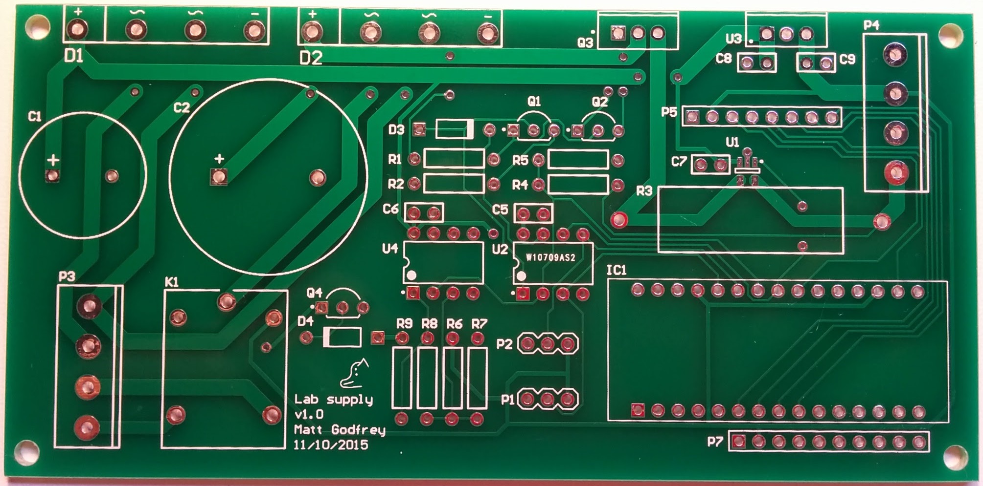
This necessitated a complete re-layout and repositioning of all the components. I used this as an opportunity to place the connectors in more accessible positions and to more clearly separate the different circuits – the transformer tap select for example is now down in the bottom left, right next to the relay. I also fixed a problem with the footprint for the 4 terminal phoenix connector which didn’t have any pads on the back of the board (making it very difficult to solder!)
I also added some via stitching to all of the high current traces to increase the current handling capability. Each of the vias should be able to handle about 2-3A, so I have added 3 to each trace, rather than the original 1 just to be safe. This turned out to be harder than expected to do in Circuitmaker – there is probably a simple way, but I didn’t find it. I had trouble with tracks and vias disappearing as I tried to add additional vias. Apart from this minor complaint however, I’m still very impressed with Circuitmaker and recommend people give it a try.

Finally, I added a jumper (J1) to the current limiting path so that it can be disabled easily for testing. This was actually already useful in debugging the problem with (another!) blown current monitor chip when I built this circuit up.
Cosmetic
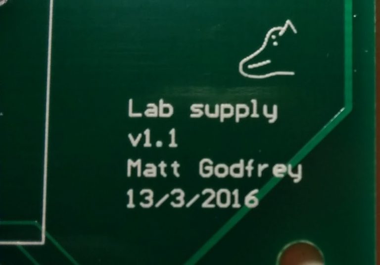
I added some labeling to the input and output terminals on the silkscreen. I also changed the amber gambler logo into a font, as described in this blog post. This makes it simpler to re-size and add to new designs.
Summary and next steps
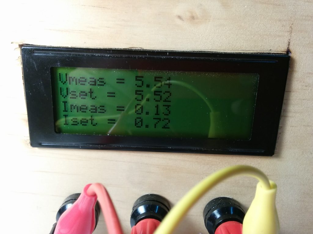
The board has gone through some simple electrical testing and seems to be working nicely. The voltage and current limiting are working properly – I would like to test this over some more load conditions though. The LCD displays both the setpoint and measured values for the current and voltage and has been software calibrated. I still need to try to do some measurements of the noise/ripple under different load conditions, and to test the stability of the output over time and as it heats up.
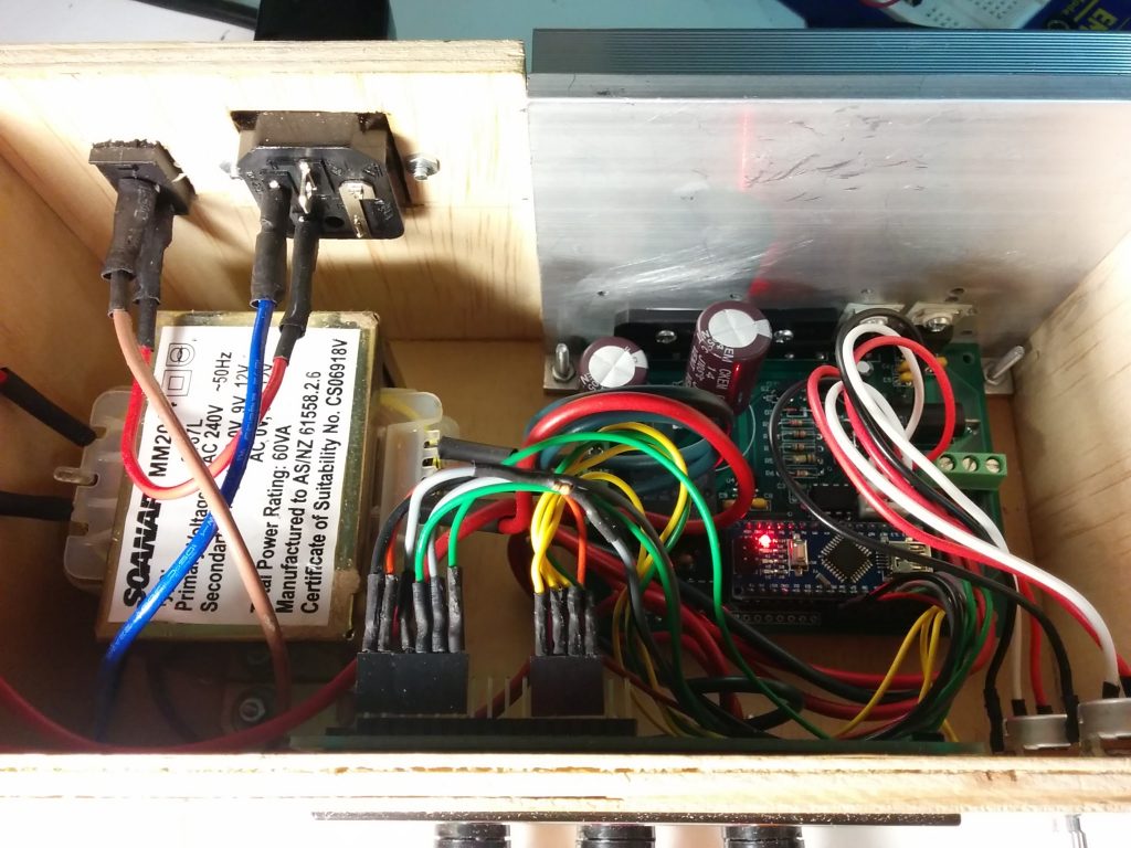
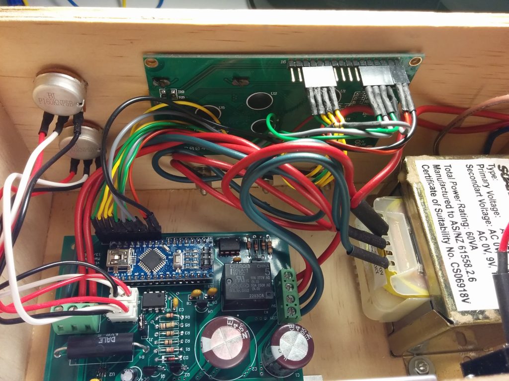
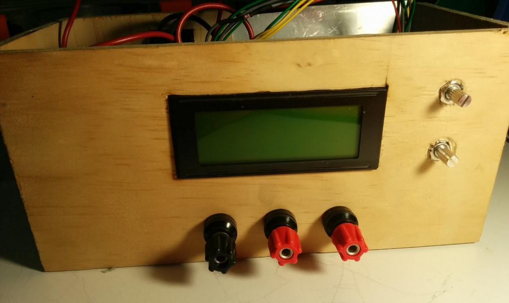
The enclose us mostly complete with the transformer, PCB, heatsink, mains input and front panel items all installed. It just needs a top for the box, a coat of paint or lacquer and some knobs for the pots to finish it off.
Further improvements/modifications:
- Add the contrast set resistor for the LCD to the PCB – at the moment it is soldered in-line
- Add pins for (and trimpot to adjust) the LCD backlight – it is currently not connected.
- More labeling of the board – for example, voltage and current set pot connectors, LCD pin names on connector.
- Replace the Arduino with just the AVR microcontroller. I can still install the Arduino bootloader on the chip, but there is no need for the full Arduino board on there – it was just a convenience.
- Investigate current handling capability of the thermal reliefs for ground pads on high current pins – they seem very thin…

- Simulate the feedback loop to determine phase margin and stability
- Add some test points and additional jumper/0 Ohm resistors to the board for easier debugging

